대표어
대표어

권호기사보기
| 기사명 | 저자명 | 페이지 | 원문 | 기사목차 |
|---|
결과 내 검색
동의어 포함
표제지
목차
국문초록 10
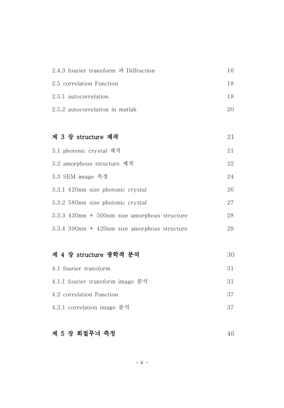
제1장 서론 11
제2장 이론 14
2.1. LED 추출효율 14
2.1.1. LED 추출효율 정의 14
2.1.2. LED 내부 전반사 16
2.1.3. LED 추출효율을 향상시키는 방법 18
2.2. photonic crystal 20
2.2.1. photonic crystal 특징 20
2.3. amorphous structure 21
2.3.1. amorphous structure의 특징 21
2.4. fourier transform 23
2.4.1. 1차원 fourier transform 23
2.4.2. 2차원 fourier transform 25
2.4.3. fourier transform과 diffraction 26
2.5. correlation 28
2.5.1. autocorrelation 28
2.5.2. autocorrelation in matlab 30
제3장 structure 제작 31
3.1. photonic crystal 제작 31
3.2. amorphous structure 제작 32
3.3. FE-SEM image 측정 34
3.3.1. 420㎚ size photonic crystal 36
3.3.2. 580㎚ size photonic crystal 37
3.3.3. 420㎚ + 500㎚ size amorphous structure 38
3.3.4. 390㎚ + 420㎚ size amorphous structure 39
제4장 structure 광학적 분석 40
4.1. fourier transform 41
4.1.1. fourier transform image 분석 41
4.2. correlation 47
4.2.1. correlation image 47
제5장 회절무늬 측정 56
5.1. blue laser의 beam Size 측정 57
5.2. CCD Camera로 회절무늬 측정 60
제6장 결론 64
참고문헌 66
Abstract 71
그림 2-1. 칩 내부에서 발생하는 내부 전반사 현상 17
그림 2-2. 다양한 기하학적 구조의 LED 19
그림 3-1. FE-SEM S-4300 35
그림 3-2. 420㎚ photonic crystal (silicon) 36
그림 3-3. 580㎚ photonic crystal (silicon) 37
그림 3-4. 420㎚+500㎚ amorphous structure (silicon) 38
그림 3-5. 390㎚+420㎚ amorphous structure (silicon) 39
그림 4-1. 420㎚ SEM image의 fourier transform image 41
그림 4-2. 확대이미지 41
그림 4-3. 580㎚ SEM image의 fourier transform image 43
그림 4-4. 그림 4-4의 확대한 이미지 43
그림 4-5. 420㎚+500㎚ SEM image의 fourier transform image 45
그림 4-6. 390㎚+420㎚ SEM image의 fourier transform image 46
그림 4-7. hexagonal ideal image 47
그림 4-8. ideal image의 correlation image 48
그림 4-9. ideal image의 correlation peak 그래프 49
그림 4-10. 420㎚ SEM image의 correlation image 50
그림 4-11. 580㎚ SEM image의 correlation image 50
그림 4-12. photonic crystal correlation 값 그래프 51
그림 4-13. 지수함수 fitting 그래프 52
그림 4-14. 420㎚+500㎚ SEM image의 correlation image 53
그림 4-15. amorphous structure의 correlation peak 그래프 54
그림 4-16. 지수함수 fitting 그래프 55
그림 5-1. beam intensity peak 값 그래프 57
그림 5-2. error function graph 58
그림 5-3. 580㎚ photonic crystal의 회절무늬 60
그림 5-4. 420㎚+500㎚ amorphous structure의 회절무늬 62
*표시는 필수 입력사항입니다.
| 전화번호 |
|---|
| 기사명 | 저자명 | 페이지 | 원문 | 기사목차 |
|---|
| 번호 | 발행일자 | 권호명 | 제본정보 | 자료실 | 원문 | 신청 페이지 |
|---|
도서위치안내: / 서가번호:
우편복사 목록담기를 완료하였습니다.
*표시는 필수 입력사항입니다.
저장 되었습니다.