대표어
대표어
 학술연구정보서비스(KERIS)
권호기사보기
| 기사명 | 저자명 | 페이지 | 원문 | 기사목차 |
|---|
결과 내 검색
동의어 포함
title page
Abstract
Contents
CHAPTER 1. Introduction 14
1.1. Structural Stability 14
1.2. Surface Magic Cluster 16
1.3. Outline of Thesis 18
CHAPTER 2. Theoretical Methods 20
2.1. Density Functional Theory 20
2.2. Density Functional Perturbation Theory 24
2.3. Plane Wave Pseudopotential Method 26
2.4. Outline of DFT Codes 32
2.4.1. WIEN2k 32
2.4.2. VASP 34
2.4.3. ABINIT 35
2.4.4. CPMD 36
2.4.5. SIESTA 37
CHAPTER 3. Ab initio study of thallium nanocluster on Si(111)-7x7 49
3.1. Introduction 49
3.2. Calculation Details 50
3.3. The Adsorption of Group III Elements on Si(111)-1x1 52
3.4. The Adsorption of Group III Elements on Si(111)-7x7 53
3.4.1. The Energy of Single Atom Adsorption 53
3.4.2. Magic Clusters of Al, Ga, In 57
3.4.3. Thallium Cluster 60
3.4.4. Electronic Band Structures 68
3.5. Conclusions 75
CHAPTER 4. Summary 76
Appendix 78
Appendix A. Ab initio P-T phase diagram of NaBH₄ 78
Appendix B. Verification of topological crossings in band structure of solids 97
References 118
요약문 128
감사의 글 130
Curriculum Vitae 131
Fig. 2.1. Flow-chart depicting a generic Kohn-Sham calculation 21
Fig. 2.2. Partitioning of the unit cell into atomic spheres (I) and an interstitial region(II) 32
Fig. 2.3. Measured computing times (in seconds) of pdsygvx routine for 1-dimensional and 2-dimensional processor grids. The grids are 2x2, 2x4, and 4x4 for the number of cpus 4, 8, and 16, respectively, in the 2-dimensional grid. 41
Fig. 2.4. GaAs bulk band structure calculated with SIESTA taking into account spin-orbit coupling. 45
Fig. 2.5. Thallium bulk band structure calculated with SIESTA taking into account spin-orbit coupling. Dots by PP-LAPW (WIEN97) method are also shown to check our results.... 48
Fig. 3.1. Side view of the calculated unit cell of Si(111)-7x7. 51
Fig. 3.2. (a) The energy of a single group III metal atom (Al, Ga, In, Tl) adsorption at the attractive basin of Si(111)-7x7. (b) Symmetric adsorption sites around the rest atom which belongs to the faulted-half unit cell.... 54
Fig. 3.3. Top view of a single metal atom adsorption on the faulted-half unit cell of Si(111)-7x7, where the metal atom is placed at the edge adatom site with a displacement of the Si adatom.... 56
Fig. 3.4. Top view of triangular shape cluster of Al, Ga, In on the faulted-half unit cell of Si(111)-7x7. The cluster consists of six metal atoms. The symbol has the same meaning as Fig. 3.3. 58
Fig. 3.5. Top view of most stable cluster of Al, Ga, In,71 for (a) N=5 and (b) N=7 (see the text). The symbol has the same meaning as Fig. 3.3. 59
Fig. 3.6. The adsorption energies given by (a) Eq. (3.2) and (b) Eq. (3.3), of thallium clusters for 1 ≤ N ≤ 10, where N is the number Tl atoms within the cluster. See the text for the meaning of configuration symbol in (a).... 62
Fig. 3.7. Top view of Tl clusters on the faulted-half unit cell of Si(111)-7x7 with the lowest energy for each N. The symbol has the same meaning as Fig. 3.3. 63
Fig. 3.8. Potential energy surfaces of the thallium atom at 5.5 Å above the Si(111)-2x2 surface layer for (a) the unfaulted clean surface and (b) the faulted surface with one thallium atom adsorbed at the most stable site.... 66
Fig. 3.9. (a) Energy barrier for the rotation of three Tl adatoms which are indicated by gray rectangles in (b), (b) top views of each configurations. ΔE for a→b→a' (through hollow site) and a→c→a' (through top site) are 0.03 and 0.02 eV/Tl,... 67
Fig. 3.10. Surface band structures of (a) the clean 7x7 surface, (b) Al, (c) Ga, (d) In clusters on it. Black dots represent surface states localized in top three surface layers including Si adatoms.... 69
Fig. 3.11. Projected density of states of (a) the clean 7x7 surface, (b) Al, (c) Ga, (d) In clusters on it. The radii used to project a wavefunction inside atomic spheres are the same in the all plots.... 70
Fig. 3.12. Projected density of states of (a) 3B-3B-3B, (b) T2B-T2B-T2B thallium clusters on Si(111)-7x7 surface. {Fa,Un}{Re,Ad}-Si, Tl mean {faulted,unfaulted} silicon {rest atoms,adatoms}, nine thallium adatoms.... 72
Fig. 3.13. Surface band structure for the configuration of (b) in Fig. 3.12. Black and open dots represent surface states localized in top three surface layers and thallium atoms, respectively.... 73
Fig. 3.14. Electronic energy level changes with the increase in thallium coverage by the photoemission experiment (left) and by our calculation (right). 74
Fig. A.1. NaBH₄ structures (large yellow : Na, middle blue : B, small red and green : H) : (a) two different configurations (indicated by red and green colors) of [BH₄]- in disFCC phase (Fm3m)...(이미지참조) 86
Fig. A.2. Phonon DOS of FCC, TET, nd FCCSC. Only three energy windows (0 ~ 500, 1000 ~ 1300, 2200 ~ 2500 cm-1) are chosen, because there is no state outside these intervals.(이미지참조) 87
Fig. A.3. Total and local DOS projected on each atom for (a) FGC and (b) TET. Fermi level is set at zero energy. Atomic radius used in projected DOS is 2.0, 1.3, 1.0 for Na, B, H in unit of bohr radius. 89
Fig. A.4. (a) Born effective charge (Z*) of Na and (b) high-frequency dielectric constants (ε∞) as a function of pressure. Effective charge of BB₄ is equal to minus the Na charge and B has nearly zero charge.(이미지참조) 91
Fig. A.5. Phonon band structure and DOS of FGG phase at (a) 0 GPa, (b) 27 Gpa. 93
Fig. A.6. Phonon band structure and DOS of TET phase at (a) 0 GPa, (b) 27 GPa. 94
Fig. A.7. P-T phase diagram of NaBH₄. (a) Phase boundaries are drawn by joining transition points. To obtain the transiton points two approimations (FCC and FCCsc) for disFCC are used.... 95
Fig. B.1. Energy curves for the lowest 4-branch energy band in Ag₂Se in the y and z-directions. Γ, Y and Z are symmetry points in the Brillouin zone. Γ₁Γ₂Γ₃ and Γ₄ label the one-dimensional irreducible representations of the space group no.... 111
Fig. B.2. Same as in Fig. B.1 but for the crystal AsGeSe in x and y-directions of the Brillouin zone with the space group no. 52 Pnna. Here the topologically unavoidable crossing is in the y-direction.... 112
Fig. B.3. Same as in Fig. B.1 but for the crystal OPb with the space group no. 57 Pbcm. The topologically unavoidable crossing is in the y-direction. The crossing in the flgure in the z-direction is not required by symmetry and topology. 113
Fig. B.4. Same as in Fig. B.1 but for the crystal CMo₂ with the space group no. 60 Pbcn. The topologically unavoidable crossing is in the z-direction. 114
Fig. B.5. Same as in Fig. B.1 but for the crystal PdSe₂ with the space group no. 61 Pbca. The topologically unavoidable crossing is in the y-direction. 115
Fig. B.6. Same as in Fig. B.2 but for the crystal BFe with the space group no. 62 Pnma. There are two topologically unavoidable crossings in the y-direction. 116
*표시는 필수 입력사항입니다.
| 전화번호 |
|---|
| 기사명 | 저자명 | 페이지 | 원문 | 기사목차 |
|---|
| 번호 | 발행일자 | 권호명 | 제본정보 | 자료실 | 원문 | 신청 페이지 |
|---|
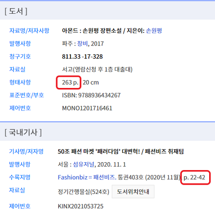
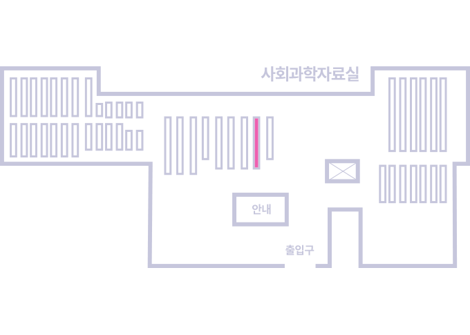
도서위치안내: / 서가번호:
우편복사 목록담기를 완료하였습니다.
*표시는 필수 입력사항입니다.
저장 되었습니다.