대표어
대표어
권호기사보기
| 기사명 | 저자명 | 페이지 | 원문 | 기사목차 |
|---|
결과 내 검색
동의어 포함
Title Page
ABSTRACT
Contents
Chapter 1. Introduction 12
1.1. Low-Dimensional Electronic Systems 14
1.2. Conventional Low-Dimensional Materials 18
1.3. Low-Dimensional Systems on Silicon Surfaces 20
1.3.1. Reconstruction of Silicon Surfaces 20
1.3.2. Surface States of 1D and 2D Systems 24
1.4. Overview 27
Chapter 2. Angle Resolved Photoelectron Spectroscopy 28
2.1. Principle of ARPES 28
2.2. Spectral Function of ARPES 35
2.3. Analysis of ARPES 40
2.4. Application from Theory to Experiment 43
Chapter 3. Experimental Details 45
3.1. Low-Temperature ARPES System 45
3.1.1. Basic Configuration of Fermi Surface Mapping System 45
3.1.2. Photon Source : He-Discharge Lamp 45
3.1.3. Sample Manipulator 49
3.1.4. Electron Analyzer 52
3.1.5. Data Acquisition and Analysis Softwares 58
3.2. Low-Energy Electron Diffraction 58
3.3. Sample Preparation 60
3.4. Other Technical Issues 67
3.5. Summary 70
Chapter 4. Electron-Phonon Interaction of 1D and 2D Surface States in Indium Adlayers on the Si(111) Surface 71
4.1. Introduction 71
4.2. Experimental Methods 81
4.2.1. Sample Preparations 81
4.2.2. ARPES Measurements 82
4.3. Electronic Structures of the In/Si Interfaces 83
4.3.1. Overall Band Dispersions 83
4.3.2. Determination of EPC Constant λ 86
4.4. Origin of the Enhanced EPC 91
4.5. Summary 96
Chapter 5. Observation of Metal-Insulator Transition on Si(111)4 × 1-In surface with Oxygen Defects 98
5.1. Introduction 98
5.2. Experimental Methods 102
5.3. LEED Results 103
5.4. Structure Models 106
5.5. Electronic Structures on Si(111)4 × 1-In Surface with Oxygen Defects 108
5.5.1. Observation of MIT 110
5.5.2. Electron Doping Effects 112
5.6. Discussion : Origin of MIT with Increased Tc(이미지참조) 114
5.7. Summary 118
Chapter 6. Conclusion 119
References 121
Summary 130
Curriculum Vitae 134
Figure 1.1: Schematic illustrations of the density of states (left column), band dispersion (center column) and Fermi surfaces (right column) of (a) three-dimensional, (b) two-dimensional, (c) one-dimensional and (d) zero-dimensional free-electron systems. 13
Figure 1.2: (a) Simple visualization of strong interactions between electrons in a 1D system. Electrons cannot escape from each other when moving along a line, which leads to the formation of collective excitations and the breakdown of the single electron picture.... 15
Figure 1.3: Overview of CDWs in a ID atomic chain with a half electron filling. The red balls are the atoms consisting of the 1D chain. The lines above the balls represent charge densities. The bottom part shows the respective band dispersions of 1D free electrons in the given lattice... 16
Figure 1.4: (a)The Lindhard susceptibility of free-electron gases in one-, two-, and three-dimensions. (b) The Lindhard susceptibility of a hexagonal Fermi surface(χhex) is compared the 1D(χ1D) and 2D(χ2D) free electron case....(이미지참조) 17
Figure 1.5: Cartoons showing the prototypical examples of low-dimensional materials. 19
Figure 1.6: Schematic illustrations for various surface reconstructions: 21
Figure 1.7: STM images for various low-dimensional structures realized on Si(111) with metal adsorbates. 23
Figure 1.8: (a) Simplified 1D model of a periodic crystal potential terminating at an ideal surface. At the surface the model potential jumps abruptly to the vacuum level (solid line). The dashed line represents a more realistic picture, where the potential reaches the vacuum level... 25
Figure 1.9: (a) Fermi surfaces and band dispersions for the 2D structures on Si(111). A surface state band can be doped continuously by excess Ag or Au atoms on top of the stoichiometric Si(111) √3×√3-Ag structure.... 26
Figure 2.1: Geometry of an ARPES experiment in which the emission direction of the photoelectron is specified by the polar (θ) and azimuthal (Φ) angles 29
Figure 2.2: Schematic view of the photoemission process in the single particle picture. The electron energy distribution produced by incoming photons and measured as a function of the kinetic energy Ekin of the photoelectrons (right) is more conveniently expressed in terms of the...(이미지참조) 31
Figure 2.3: Illustration of the three-step model, with (1) optical excitation of an electron in the bulk, (2) transport of the photoelectron to the surface, and (3) escape of the photoelectron into vacuum free space. 33
Figure 2.4: Angle-resolved photoemission spectroscopy: 36
Figure 2.5: Simulation of A(k,ω) using a model self-energy. The solid and dashed lines show A(k,ω), and the coherent quasiparticle peak which was linearly expanded around Ek*, respectively....(이미지참조) 38
Figure 2.6: Energy (ω) vs momentum (kII) image plot of the photoemission intensity from Bi₂Sr₂CaCu₂O8+δ along (0,0)-(π,π). This k-space cut was taken across the Fermi surface (see sketch of the 2D Brillouin zone upper left) and allows a direct visualization of the photohole...(이미지참조) 41
Figure 2.7: Series of EDCs for the surface state of Be(0001) near EF taken at 15 K. The spectral functions calculated for the corresponding emission angles (solid lines) are compared. The dispersion shows the unusual lineshapes due to electron-phonon coupling.(이미지참조) 42
Figure 2.8: Illustration of the effects of electron-phonon coupling. 43
Figure 3.1: Basic configuration of the Fermi surface mapping system 46
Figure 3.2: (a) Schematic drawing of VUV source head (VG-Scienta, Sweden). (b) Graph showing the relative intensities of multiple emissions from the He-discharge lamp (see text). The spectra were measured on the Al photodiode with a bias of -15 V.... 48
Figure 3.3: Pictures taken for the ARPES station equipped with the high-performance Scienta electron analyzers and high-flux He-discharge sources 49
Figure 3.4: CAD drawing of the low-temperature manipulator. The sample temperature can be cryogenically cooled down to 88 K. (b) Continuous measurement of the band dispersion of the oxygen-induced surface at various temperatures, using the manipulator shown in (a). 50
Figure 3.5: Temperature of manipulator as a function of time after LN2 injection. 51
Figure 3.6: Various methods of temperature calibration. 53
Figure 3.7: Geometry requirement for ARPES system. Probing point of the electron analyzer is one point in the space. Every rotational axis, surface of sample and beam path should be aligned to pass through the point. 54
Figure 3.8: (a)CAD drawing of SES R4000 electron analyzer (VG-Scienta, Sweden). (b) Schematic drawing of the internal structure of the analyzers. They can be categorized into three parts; the lens, hemispheres, and detector plates.... 56
Figure 3 9: Data acquisition and analysis softwares (a) SES, (b) Igor Pro, and (c) SES sequence manager. 57
Figure 3.10: (a) LEED apparatus. Electrons thermally emitted from the filament are focussed onto the sample. Elastically scattered electrons are passed by the grids and accelerated onto the fluorescent collector grid.... 59
Figure 3.11: Schematic illustration of the Knudsen-type cell evaporator (home-made). 61
Figure 3.12: Temperature calibration with a silicon test sample. We found a linearity between wafer temperature and heating current in the semi-log plot. The sample temperature was recorded with an optical pyrometer.... 62
Figure 3.13: Heat treatment diagram applied for flash heating of Si samples in UHV. 63
Figure 3.14: LEED patterns of (a) the clean Si(111)7×7 and (b) √3×√3-In surface for estimation of the coverage 1/3 ML, (c) √31×√31-In surface, (d) 4×1-In surface for estimation of the coverage 1 ML, (e) √7×√3-In surface. 64
Figure 3.15: Surface phase diagram of In adsorption on Si(111) for temperatures of 500-600 K 65
Figure 3.16: LEED patterns for In adsorption on the Si(111)√3×√3-In surface at room temperature. 66
Figure 3.17: Photoelectron intensity map of the Si(111)6×6-In surface (a) at EB=1.0 eV, (b) 0.5 eV, and (c) Fermi energy at 90 K.(이미지참조) 69
Figure 4.1: A photoemission band dispersion diagram of Si(111)√3×√3-Ag at Γ point. (b) Energy distribution curves (EDCs) with the fitted (red) and Gaussian-convoluted Lorentzian (black) curves....(이미지참조) 72
Figure 4.2: (a) Zigzag model for Si(111)4×1-In at RT. (b) Hexagon model for Si(111)8×2-In at low temperature. The dimerization and shear movements during the (4×1 ↔ 8×2 phase transition) are indicated by the arrows.... 73
Figure 4.3: (a) Fermi surface for Si(111)4×1-In at RT (b) underlying band dispersions at RT(above Tc, left) and at 45K(below Tc, right).(이미지참조) 74
Figure 4.4: STM images of the √7×√3-In structures. 75
Figure 4.5: (a) STM topograph and (b) Fermi surfaces and band dispersions of Rec Si(111) √7×√3-In surface. (c) The tunneling conductance and superconducting gap for Rec Si(111)√7×√3- In surface. 76
Figure 4.6: (a) Quantum size effect : Monolayer thickness-resolved normal-emission photoemission spectra of the Pb thin films measured in situ at 75 K. (b) STM images of two types of 2-ML Pb films (I : 1×1, II : √3×√3) (c) Conductance spectra acquired at various temperatures for... 78
Figure 4.7: (a)The differential conductance of single-particle tunneling measured with Nb tip on the striped incommensurate (SIC)-Pb phase as a function of temperature. The curves at different temperatures are offset vertically for clarity.... 80
Figure 4.8: LEED patterns of (a) 4×1-In and (b) √7×√3-In surfaces. 82
Figure 4.9: Schematics of the structure models for the √7×√3-In surface with (a) 2.4 ML as proposed recently and (c) 1.2 ML (the so called rectangular √7×√3 model) and the widely accepted model (1.0 ML) for (b) the 4×1-In surface.... 83
Figure 4.10: Electronic structures of the In double layer Si(111). 84
Figure 4.11: Schematics of Fermi contours for the Si(111)√7×√3-In and (b) 4×1-In surfaces. The corresponding band dispersions (ARPES intensity maps in color scale) measured along the red lines in (a) and (b) at 130 K are displayed in (c) and (d), respectively.... 86
Figure 4.12: Selected ARPES energy distribution curves for different surface states at different kx indicated by arrows in Figures 4.11(c) and (d) taken at 130 K. These curves are fitted with multiple Lorentzian functions as shown in the Figure 4.12 and the Fermi-Dirac function and...(이미지참조) 88
Figure 4.13: The Lorentzian energy widths of the surface states of the (a) √7×√3-In and (b) 4×1-In surfaces are plotted as a function of temperature. From the linear fit of each set of data the corresponding electron-phonon coupling constant λ was obtained as indicated.... 89
Figure 4.14: Simulations of band dispersion on the surface states of the (a) m₃ and (b) ss states. Accurate band dispersion is used the calculation of DOS. 92
Figure 5.1: STM images for (a) Co and (b) Pb on Si(111)4×1-In surface 99
Figure 5.2: (a) STM image of the Na-added Si(111)4×1-In surface at RT. The intensity profiles along the line AB (the 4×2 domain) and the line CD (the 4×1 domain) are plotted to show the period doubling by Na adatoms.... 101
Figure 5.3: LEED patterns of 8×2-In surface at (a) 110 K, and (b) 120 K. (c) LEED pattern of 4×1-In surface at 130 K. Temperature dependence of LEED patterns for the pristine 4×1-In surface is almost same the 4×1-In surface with oxygen exposure below 150 K. 104
Figure 5.4: LEED patterns of the oxygen-induced surface as a function of sample temperature. The intensities of streak [indicate a white dashed arrow] and ×8 spot [indicated a white solid arrow] are weakened as temperature increases, and finally disappear at 180 K. 105
Figure 5.5: Intensities of the ×8 diffraction spot and photoelectron intensities of folded state as a function of the sample temperatures for the oxygen-induced surface with 6 L exposures at RT and LT.... 106
Figure 5.6: Structural characterizations of 4×1-In and 8×2-In surfaces. Atomic structural models of the (a) 8×2-In and (b) 4×1-In surfaces. Red and black balls indicate In and Si atoms, respectively.... 107
Figure 5.7: Structure model suggested by potential energy surface calculated for oxygen adatoms on the Si(111)4×1-In surface. Large (red) and small (black) balls indicate In and Si atoms, respectively.... 108
Figure 5.8: The temperature-dependent ARPES measured the oxygen-induced surface with 6 L exposures along K-M-K' direction a function of sample temperaure. The folded state vanished at increasing Tc, around 170 K....(이미지참조) 109
Figure 5.9: EDCs to confirm double gap structures. These EDCs is extracted at selected k points [indicated white arrows] in Figures 5.6(e) and 5.8 at 120 K. We confirmed that pristine 4×1-In surface is similar to oxygen-induced surface with double gap structure while band gap... 110
Figure 5.10: (a) MDCs as a function of substrate temperature at black dashed line in Figure 5.8. These curves are fitted with multiple Lorentzian functions (shown in the figure). The solid lines indicate the Lorentzian fitting results on the raw data in open circles.... 111
Figure 5.11: (a) MDCs as a function of various oxygen exposures at Fermi energy. (b) EDCs at peak positions of these curves (red dashed line) in Figure 5.8 (a). This spectra are measured at 300 K. 113
Figure 5.12: Representative STM images from H-adsorbed and oxygen-adsorbed indicated as a circle and a square. On the oxygen-adsorbed surface, the dark features dominantly appear while the bright features are minor. 115
Figure 5.13: Representative STM images from O-adsorbed surface with different exposure, (a) 3 L and (b) 10 L at 140 K. On the oxygen-adsorbed surface, the dark features dominantly appear while the bright features are minor consistent with previous Figure 5.12.... 116
저차원 전자구조를 갖는 물질계는 흥미로운 물리현상을 보여줄 뿐만 아니라 극소형 전자소자를 위한 응용성 때문에 최근 수십년간 지속적인 연구와 관심의 대상이 되어왔다. 특히 저차원 전자계는 일반적인 3차원 물질들에는 존재하지 않거나 쉽게 관측이 되지 않는 여러가지 흥미로운 물리현상을 관찰할 수 있다는 장점을 가지고 있다. 기존에 많이 연구되어지던 이방성이 큰 3차원 물질계에 더하여. 최근에는 반도체 표면위에 자기 조립되는 다양한 형태의 1차원 원자막선과 2차원 원자막들이 새로운 저차원 전자계로 주목 받고 있다. 실제로 이러한 물질계는 뚜렷한 저차원 전자구조를 갖고 있으며, 스핀/전하 밀도파, 비페르미액체현상 그리고 질량이 없는 디락입자와 같은 흥미로운 저차원 물리현상들을 보여주었다.
표면에 형성된 나노구조물들의 가장 큰 장점 중 하나는 이 물질계의 특유의 다양성이라고 할 수 있다. 나노구조를 형성하는 물질의 배합이나 화학성분량을 조절하여 서로 다른 구조와 주기를 갖는 다양한 저차원상들을 체계적으로 유도해 낼 수 있다. 그 대표적인 예로 실리콘 (111) 표면 위에 자기 조립되는 원자 한층 두께의 “2차원 인듐 원자막”과 “1차원 인듐 원자선”을 들 수 있다. 다시 말해, 매우 적은 인듐 원자량에 의해 민감하게 의존하여 많은 규칙적인 상들이 나타나며, 이들은 서로 다른 주기와 형태의 전자구조를 가지고 있다. 실제로 “1차원 인듐 원자선”의 경우, 상온에서 안정적인 일차원 금속 전도성을 보여주지만 130K 아래의 저온에서는 비금속 전도성을 가지는 현상일 일어날 뿐 아니라 구조적인 변화도 같이 일어나게 된다. 그리고 “1차원 인듐 원자선”에 불순물을 주입하여 전자구조를 바꿀 수도 있다. 그리고 “2차원 인듐 원자막”의 경우에는 극저온에서 2차원 전자구조를 가지며 극저온에서 초전도성을 가지게 된다. 이와 같이 실리콘 기판위에 형성되는 인듐 원자선/원자막계에 다양한 구조를 가지는 여러가지 상들이 존재하며, 이러한 특유의 구조적 “다양성”은 곧 그에 대응하는 다양한 전자구조를 체계적으로 연구할 수 있는 좋은 기회를 제공한다.
위와 같은 배경을 바탕으로, 본 학윈 논문에서는 고분해능 각도분해 광전자 분광법을 활용하여 인듐 원자선/원자막 그리고 인듐 원자선과 불순물과의 반응으로 일어나는 전자구조를 연구하였다. 첫째로 인듐 원자막과 인듐 원자선의 광전자 분광 연구 결과, 온도가 감소함에 따라 밴드의 두께가 줄어듬을 확인하였고, 이 두께는 전자와 포논의 상호작용에 큰 영향을 미치게 된다. 인듐 원자막의 경우, 이전에 보고된 것처럼 비슷한 값을 가지게 되지만, 인듐 원자선의 경우는 표면에서 관찰된 값 중에 가장 큼을 확인할 수 있다. 이 둘의 차이는 페르미면의 차원이 1차원에서 2차원, 3차원으로 확장되면서 전자와 포논 상호작용은 점점 줄어들게 되며, 이것은 상태밀도에 비례하게 된다. 이로써 관측된 표면 전자 밴드 구조는 전자와 포논의 역활이 굉장히 중요하다는 것을 알아냈다.
둘째로 원자선 위에 흡착된 불순물의 경우, 불순물의 종류와 온도에 따라 다른 구조를 가지고 있다. 나트륨, 수소, 인듐 등은 원자선 위에 흡착되어 130K 아래에서도 원자선이 가지는 상온의 구조를 가지고 있다. 그러나 산소 흡착의 경우, 위와 반대로 130K 위에서도 원자선이 가지는 저온의 구조를 가지고 있다. 이것의 전자구조를 알아보기 위해 고분해능 광전자 분광법을 이용하여 실험한 결과, 산소 흡착의 경우는 구조적 인 변화뿐만 아니라 전기적으로도 변화를 일으키게 되며, 이때 비금속성이 나타나게 된다. 또한 이 증가된 전이온도는 산소 불순물이 비금속 전도성을 가지는 바닥상태를 산소가 더욱 더 안정화시키게 되면서 기존이 원자선이 가지는 구조를 가지게 되는 것으로 볼 수 있다. 기존의 원자선이 가지는 바닥 상태에서의 구조는 포논의 역활이 굉장히 중요한데 이 포논의 역활을 산소 불순물이 더 활성화시키는 것이다.
종합하면, 원자선과 원자막 그리고 불순물과의 상호작용에는 전자와 포논의 상호작용이 굉장히 중요하게 되며, 이러한 다체계 상호작용은 전하 밀도파, 초전도성 등과 같은 저차원 물리현상을 야기시키며, 더 많은 이론적, 실험적 연구가 진행되어야 할 것이다.*표시는 필수 입력사항입니다.
| 전화번호 |
|---|
| 기사명 | 저자명 | 페이지 | 원문 | 기사목차 |
|---|
| 번호 | 발행일자 | 권호명 | 제본정보 | 자료실 | 원문 | 신청 페이지 |
|---|
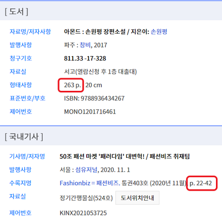
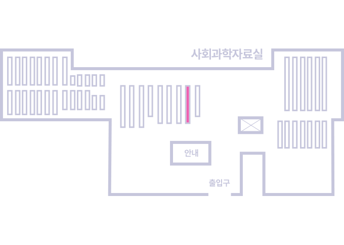
도서위치안내: / 서가번호:
우편복사 목록담기를 완료하였습니다.
*표시는 필수 입력사항입니다.
저장 되었습니다.