대표어
대표어


권호기사보기
| 기사명 | 저자명 | 페이지 | 원문 | 기사목차 |
|---|
결과 내 검색
동의어 포함
title page
ABSTRACT
Contents
Chapter 1. Introduction 12
1.1. Technology Trend 12
1.1.1. T-DMB 12
1.1.2. System-in-Package(SiP) 15
1.2. Challenges in T-DMB Stacked SiP Design 16
1.3. Research Objectives 18
1.4. Organizations 18
Chapter 2. Performance of T-DMB Receiver System in Sip 19
2.1. T-DMB Signal Demodulation Process 20
2.2. Noise Sources and Thier Modeling 20
2.2.1. Clock Noise 20
2.2.2. I/O Noise 23
2.2.3. Additive White Gaussian Noise 28
2.3. Noise Induced by Clock and I/O 29
2.3.1. Estimation of Amount of Coupling 29
2.3.2. Induced Noise On the Victim RF Line 30
2.4. Analysis of Coupled Noise's Effect 32
2.4.1. T-DMB Transmission System 32
2.4.1.1. OFDM 32
2.4.1.2. DQPSK 33
2.4.2. Demodulation Process 34
2.4.2.1. Demodulation without Noise 34
2.4.2.2. Demodulation Process with Clock Noise 36
2.4.3. Acceptable Level of Noise Coupling 41
2.4.3.1. Acceptable Level of Clock Noise Coupling 41
2.4.3.2. Acceptable Level of I/O Noise Coupling 46
Chapter 3. T-DMB Stacked SiP Design 49
3.1. SiP Overview 49
3.1.1. Die Information 49
3.1.2. Package Information 50
3.2. T-DMB Stacked SiP Design 51
3.2.1. Die Orientation 52
3.2.2. Signal's Reference 54
3.2.3. Power and Ground Distribution 56
3.2.4. Signal Grouping 57
3.2.5. Ballmap Design 58
3.3. Post-Layout Simulation 59
Chapter 4. Experimental Verification 68
Chapter 5. Conclusions 70
References 71
Summary in Korean(국문요약) 74
Acknowledgment(감사의 글) 76
Figure 1. World-widely spreading T-DMB 14
Figure 2. Expected T-DBM market growth 14
Figure 3. Comparison of SoC and SiP 15
Figure 4. Cross-sectional view of T-DMB stacked SiP 17
Figure 5. Clock signal model 21
Figure 6. Clock signal model in the frequency domain 23
Figure 7. Random NRZ data 24
Figure 8. Autocorrelation function of random NRZ data 26
Figure 9. Power spectral density of random NRZ data 27
Figure 10. Simulation to find coupling coefficients 29
Figure 11. OFDM transmission 32
Figure 12. Constellation Diagram for QPSK with Gray coding 33
Figure 13. Distortion by coupled clock noise represented on the signal space 38
Figure 14. Gray-coded quadrature phase-shift keying 40
Figure 15. Simulated BER of kth subcarrier according to coupled clock's noise 41
Figure 16. Spread of symbols' locations when Gaussian noise is considered 42
Figure 17. Simulated BER of kth subcarrier according to coupled clock's noise when Gaussian noise is considered 43
Figure 18. BER over a channel as level of coupled clock noise increases 44
Figure 19. Stack structure of T-DMB stacked SiP 50
Figure 20. Die orientation in the previous design 53
Figure 21. Die orientation in the proposed design 53
Figure 22. Electric field with and without reference at a signal line 55
Figure 23. Digital power and ground of T-DMB stacked SiP 57
Figure 24. Signal grouping 58
Figure 25. Noise coupling between Band-3 RF input signal and digital clocks in the previous design 60
Figure 26. Noise coupling between Band-3 RF input signal and digital clocks in the proposed design 61
Figure 27. Noise coupling between L-Band RF input signal and digital clocks in the previous design 62
Figure 28. Noise coupling between L-Band RF input signal and digital clocks in the proposed design 63
Figure 29. Noise coupling between Band-3 RF input signal and digital I/Os in the previous design 64
Figure 30. Noise coupling between Band-3 RF input signal and digital I/Os in the proposed design 65
Figure 31. Noise coupling between L-Band RF input signal and digital I/Os in the previous design 66
Figure 32. Noise coupling between L-Band RF input signal and digital I/Os in the proposed design 67
Figure 33. Measured performance for T-DMB signals in Band-3 68
Figure 34. Measured performance for T-DMB signals in L-Band 69
차세대 방송 시스템으로 T-DMB는 주목을 받고 있다. 기존의 아날로그식 TV/라디오 방송에 비해, 디지털식인 T-DMB는 수신성능이 뛰어나고 무엇보다 휴대용기기로 작게 구현하는 것이 가능하여 언제 어디서나 개인 단말기를 이용해 TV를 시청할 수 있는 길을 열었다. 한편, SiP기술은 이런 휴대용 T-DMB 수신시스템을 구현하는 기술로 각광받고 있다. Stacked-SiP는 기존의 SiP기술에서 한 발 더 나아가 패키지 내에서 다이를 3차원적으로 쌓음으로써 크기를 더 많이 줄일 수 있어 Stacked-SiP 기술은 T-DMB 수신시스템을 구현하기에 매우 매력적이다.
하지만, RF수신시스템과 Baseband, A/V decoder시스템이 한 패키지내에 공존하는 혼성모드 패키지에서는, 특히 RF부분과 Digital부분을 공간적으로 분리하기 어려운 stacked-SiP의 경우에는, RF부분과 Digital부분사이에 노이즈전달이 일어나기 쉽고, 이는 RF시스템의 성능을 저하시킨다. 하지만 지금까지 이에 대해 정량적인 분석에 대한 시도와 설계에 대한 가이드라인은 없었다. 이 논문에서는 이것에 대한 정량적인 분석을 통하여 목표로 하는 수신성능을 달성하기 위해서는 RF부분과 Digital부분간의 노이즈커플링을 얼마 이하로 줄여야 한다는 가이드라인을 제시하였다.
고성능의 RF성능을 얻기 위해서는 패키지내의 RF시스템에 인접한 Digital시스템의 노이즈가 커플링되는 것을 막아야 한다. 그것을 구현하기 위해서는 여러가지를 고려해야 하는 데, stack하는 다이의 방향의 고려, 민감한 RF시그널의 레퍼런스, 커플링 될 경우 RF시스템에 심각한 영향을 주는 디지털 클럭과 noisy한 IO의 레퍼런스들에 대한 고려 등을 골자로 하는, 새로운 설계 방법론을 제시 하였다.
제시한 SiP 디자인 방법론의 유용성을 증명하기 위해서, 하나는 제안한 설계 방법대로 다른 하나는 기존 방법대로 설계한 두 가지 버전의 T-DMB stacked SiP를 제작해서 이들의 성능을 비교하여 측정하였다. 성능 비교 결과, 기존 방법으로 설계한 T-DMB stacked SiP의 수신성능이 -80dBm도 되지 않은 것에 비해, 본 논문에서 제시된 대로 설계한 SiP는 수신성능이 -90dBm이상으로 향상 된 것을 확인하였다.
이상의 결과로부터, 본 학위 논문은 T-DMB stacked SiP의 설계 방법론을 성공적으로 제시하였으며, 이는 다른 mixed-mode SiP의 설계에도 적용될 수 있어 그 가치는 더욱 더 크다.*표시는 필수 입력사항입니다.
| 전화번호 |
|---|
| 기사명 | 저자명 | 페이지 | 원문 | 기사목차 |
|---|
| 번호 | 발행일자 | 권호명 | 제본정보 | 자료실 | 원문 | 신청 페이지 |
|---|
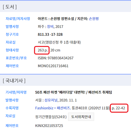
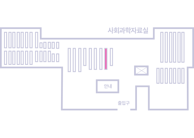
도서위치안내: / 서가번호:
우편복사 목록담기를 완료하였습니다.
*표시는 필수 입력사항입니다.
저장 되었습니다.